

Our factories: illuminating the future with chips and high-speed optical communications
Co-Pac Optics is the American distributor and U.S. division of its manufacturer. Every 1.6T OSFP224 and 800G OSFP module is engineered, coupled, and BER-verified inside our 9,600 m² optoelectronic cleanroom campus, backed by a vertically integrated compound semiconductor group.
Inside our wafer fab and optical transceiver cleanroom
Video transcript (accessible text)
- 00:00 Compound semiconductor wafers on cleanroom carriers and cleanroom engineers operating wafer metrology stations.
- 00:07 High-temperature MOCVD epitaxy chamber illumination and automated wafer stage alignment inside yellow-light cleanroom bays.
- 00:15 Optical transceiver engineering staff inspecting high-speed PCB assemblies and configuring automated optical test benches.
- 00:24 Automated cleanroom pick-and-place die bonding, active optical alignment, and trays of finished pluggable optical transceiver modules.
UPSTREAM SEMICONDUCTOR AND PHOTONIC HARDWARE
Substrates, epitaxial wafers, photonic chips and laser devices
Controlling upstream semiconductor materials and laser dies gives our optical transceiver lines direct supply continuity, tighter wavelength binning, and predictable cost structure.
 SUBSTRATES · 2" TO 6" VGF
GaAs and InP Single-Crystal Wafers
Epi-ready Gallium Arsenide and Indium Phosphide wafers engineered for high-speed data-center VCSEL, DFB, and EML epitaxial growth.
 SUBSTRATES · IR AND OPTOELECTRONICS
Germanium and Sapphire Optical Wafers
High-purity Germanium and patterned Sapphire substrates supporting multi-junction photovoltaics, infrared detectors, and photonic emitters.
 PHOTONIC CHIPS · 850 NM TO 1550 NM
VCSEL and DFB Laser Diode Chip Arrays
Single-channel and multi-channel 1x4 / 1x12 VCSEL and DFB laser arrays built for short-reach multimode and single-mode PAM4 interconnects.
 PHOTONIC CHIPS · HIGH-RESPONSIVITY RX
InGaAs PIN and MPD Photodetector Dies
Low-capacitance, low-dark-current InGaAs PIN and monitor photodiode dies for high-sensitivity optical receiver lanes and laser power monitoring.
 OPTOELECTRONIC DEVICES · TEC COOLED
Hermetic Butterfly Laser Packages
14-pin butterfly laser assemblies integrating DFB/SOA dies, thermoelectric coolers, optical isolators, and polarization-maintaining fiber pigtails.
 OPTOELECTRONIC DEVICES · TO46 / TO56
TO-CAN Lasers and Bi-Directional OSA
Hermetically welded TO46 and TO56 coaxial laser headers and TOSA/ROSA sub-assemblies for industrial, 5G fronthaul, and optical access networks.
END-TO-END MANUFACTURING FLOW
Six-stage wafer-to-transceiver production workflow
 STEP 01
Crystal Growth and Epi-Wafer Prep
VGF crystal growth, precision wire slicing, lapping, chemical-mechanical polishing, and AIX2800 G4 MOCVD epitaxial layer deposition.
 STEP 02
Photolithography, ICP Etch and Coating
Cleanroom ridge/mesa lithography, ICP dry etching, PECVD passivation, metallization, bar cleaving, and HR/AR facet coating.
 STEP 03
Automated Wafer Probing and Die Sorting
100% automated LIV, spectrum, and shear testing at wafer and bar level, with KGD mapping into serialized waffle packs.
 STEP 04
COB / Box Packaging and Active Alignment
Eutectic die attach, high-speed RF wire bonding, DSP integration, and sub-micron 6-axis silicon-photonics lens/fiber coupling.
 STEP 05
Thermal Cycling and PAM4 Eye/BER Calibration
Dynamic extinction-ratio tuning, TDECQ optimization, 0 to 70 degrees C thermal chamber stress screening, and CMIS 5.x firmware burn.
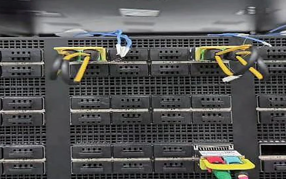 STEP 06
Switch Interop, Laser Etch and Outbound QA
Live switch port verification, custom Co-Pac Optics or white-label OEM housing laser engraving, end-face inspection, and ESD tray sealing.
ANALYTICAL AND CLEANROOM INSPECTION
Cleanroom wafer fab and analytical metrology gallery

Epi-ready GaAs and InP wafers in cleanroom cassette 
ISO Class 100/1,000 wafer and die processing bay 
Automated optical facet and die inspection 
Bruker HR-XRD epitaxial lattice metrology 
Nanometrics ECVPro carrier concentration profiling 
MOCVD epitaxial chamber and surface profilometry
CLEANROOM, EPITAXY AND METROLOGY CAPABILITIES
Six core semiconductor and optical manufacturing capabilities
From raw Group III-V crystal growth and MOCVD epitaxial wafer fabrication to 8x200G PAM4 OSFP224 transceiver burn-in, every critical stage runs under unified quality control.
VGF Single-Crystal Growth
2-inch to 6-inch compound substrates
- Vertical Gradient Freeze (VGF) growth for GaAs, InP, and Ge single-crystal ingots
- 2-inch, 3-inch, 4-inch, and 6-inch semi-insulating and semiconducting epi-ready wafers
- Low etch-pit density (EPD) and sub-nanometer CMP surface roughness for laser epitaxy
AIX2800 G4 MOCVD Epitaxy
German multi-wafer epitaxial reactors
- Production German AIXTRON AIX2800 G4 planetary MOCVD reactors for III-V multi-quantum-well structures
- 850 nm, 905 nm, 940 nm, 1310 nm, and 1550 nm VCSEL, DFB, EML, and PIN/APD epitaxial wafers
- Tightly controlled wavelength uniformity, layer thickness, and carrier doping profiles
Cleanroom Wafer Fab and Dicing
ISO Class 100 / 1,000 / 10,000 bays
- Stepper photolithography, inductively coupled plasma (ICP) dry etching, and PECVD dielectric deposition
- Rapid thermal annealing (RTA), precision wafer thinning, e-beam metallization, and optical facet coating
- Automated laser scribing, bar cleaving, 100% LIV wafer probing, and high-speed die sorting
6-Axis Silicon-Photonics Coupling
Sub-micron active optical alignment
- Automated 6-axis active waveguide-to-fiber alignment for 800G OSFP and 1.6T OSFP224 engines
- Precision flip-chip gold-tin eutectic die bonding, wire bonding, and UV/thermal epoxy curing
- Dual MPO-12/APC, MPO-16/APC, and LC optical receptacle assembly with automated end-face interferometry
Analytical Metrology Lab
Atomic-scale crystal and wafer verification
- Bruker High-Resolution X-Ray Diffraction (HR-XRD) for crystal lattice mismatch and superlattice analysis
- Nanometrics ECVPro electrochemical C-V carrier profiling and room/low-temperature Photoluminescence (PL)
- Scanning Electron Microscopy (SEM), Atomic Force Microscopy (AFM), and 3D white-light optical profilometry
7-Day Zero-Error 1.6T Burn-In
100% thermal cycling and switch qualification
- Keysight AresONE 8x200G PAM4 bit-error-rate validation with pre-FEC BER margins down to 9.2e-9
- 7-day continuous 1.6T InfiniBand loopback soak on live NVIDIA Quantum-X800 Q3400 switch ports with 0 errors
- 100% temperature-cycled burn-in (0 to 70 degrees C), CMIS 5.x EEPROM programming, and serialized test reports
Our upstream semiconductor group produces its own high-purity raw materials, VGF substrates, and MOCVD epitaxial wafers.
Per our manufacturing group's 2026 semiconductor epitaxy presentation.
Manufacturing profile and milestones
- Group Heritage
- Vertically integrated compound semiconductor group, established 2010
- 1.6T Flagship
- Launched 1.6T OSFP224 optical modules in 2025, validated over 7-day zero-error InfiniBand loopback runs
- 800G Volume Series
- Volume cleanroom shipments of high-speed OSFP optical modules since 2023
- Cleanroom & R&D
- 20+ optoelectronic industry honors and 9,600 m² active cleanroom footprint with 256+ staff (>40% R&D)verified factory cleanroom profile
Mike Clarke brings a nearly 20-year direct working relationship with our manufacturing leadership.
Leading edge innovation. Doing what most can't.
Validation, Certifications and Global Group Partners
Co-Pac Optics is the American distributor and U.S. division of its manufacturer.
Rooted at the intersection of light and semiconductor chips, we combine 15+ years of optoelectronic industrialization heritage, a 9,600 m² cleanroom campus, 256+ specialists (>40% R&D), and a vertically integrated compound semiconductor group with direct U.S. distribution and turnkey White-Label OEM execution.
Cleanroom Validation and Metrology
Every 1.6T and 800G module is burned in and BER-verified before shipment
- 7-DAY 1.6T LOOPBACK
Zero Post-FEC Bit Errors
Continuous 7-day 1.6T OSFP224 DR8 and 2xDR4 InfiniBand and Ethernet switch-fabric burn-in before shipment.
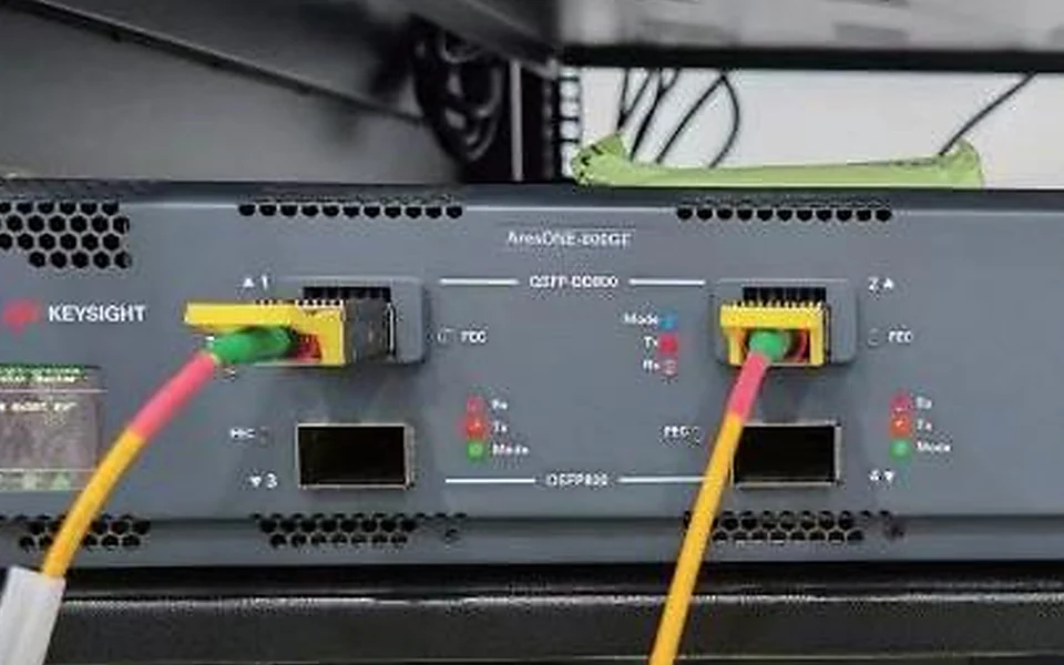 PAM4 RF AND EYE MASK
Keysight AresONE BER Suite
Per-lane TDECQ, extinction ratio, pre-FEC BER margin, and jitter verified across 8x200G and 8x100G PAM4 lanes.
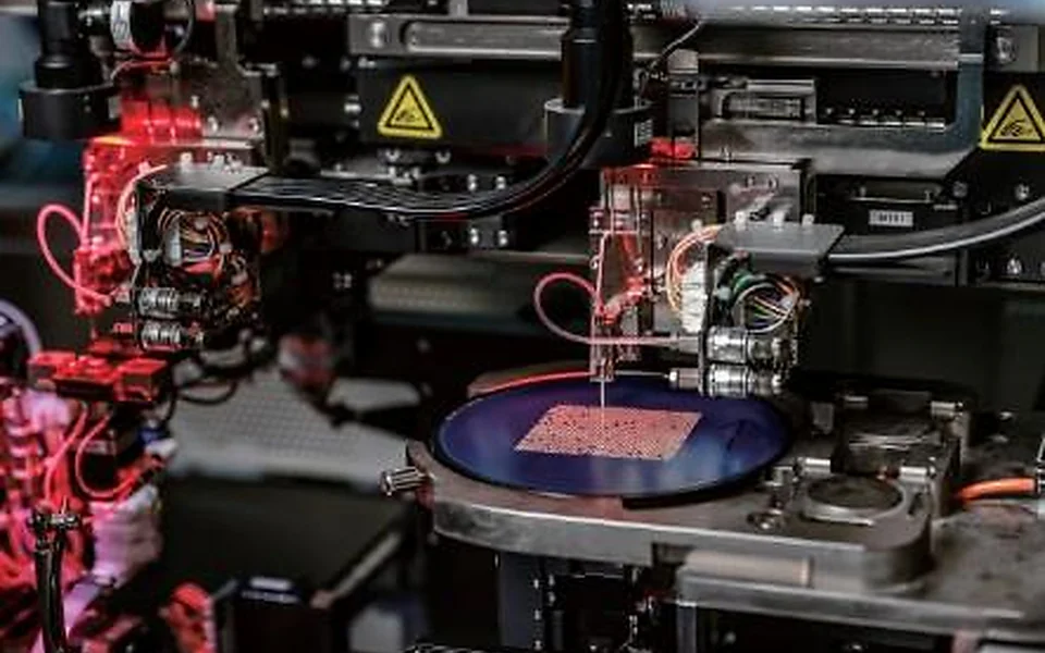 SUB-MICRON ALIGNMENT
6-Axis Active SiPho Coupling
Automated sub-micron active laser-to-waveguide alignment, UV epoxy curing, and wafer-level optical probing.
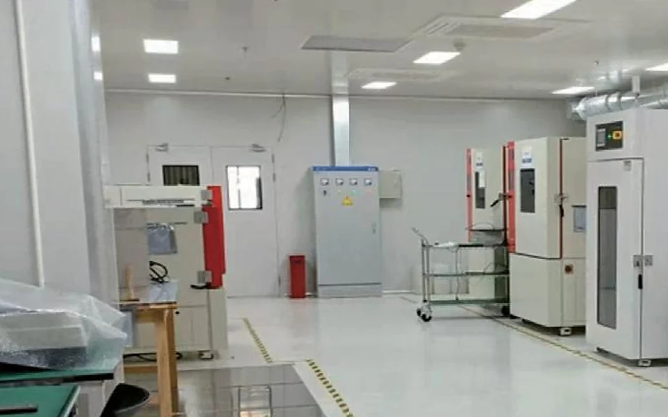 TELCORDIA QUALIFIED
Elevated Burn-In and Stress Lab
100% elevated-temperature module burn-in plus Telcordia GR-468-CORE thermal shock and 85 °C / 85% RH damp-heat life testing.
Quality, Safety and Regulatory Compliance
International certifications and optical standards
- QUALITY AND IT SYSTEMS
ISO 9001 · 14001 · 45001 · 20000-1
- ISO 9001:2015 Quality Management System (Bureau Veritas and IQC)
- ISO/IEC 20000-1 IT Service Management Certification
- ISO 14001:2015 Environmental and ISO 45001:2018 Health and Safety
- ENTERPRISE HONORS
National High-Tech and 20+ Awards
- Certified High-Tech Optoelectronic Manufacturing Enterprise
- 20+ Semiconductor, Epitaxy, and Optical Module Industry Honors
- Full MES 2D-Barcode Serial-to-Wafer Traceability
- LASER EYE SAFETY
FDA CDRH Class 1 and IEC 60825
- U.S. FDA CDRH Laser Class 1 Accession (21 CFR 1040.10)
- IEC / EN 60825-1 and 60825-2 Eye-Safe Pluggable Optics
- Automatic Tx Laser Shutdown and Fault Diagnostics
- SAFETY AND EMC APPROVALS
TÜV UL/CB · FCC · CE · VCCI
- TÜV Rheinland UL 60950-1 / IEC 62368-1 CB Scheme Safety
- FCC Part 15 Subpart B Class A/B Radiated and Conducted EMC
- CE EMC (EN 55032 / EN 55035), ICES-003 (Canada), and VCCI (Japan)
- ENVIRONMENTAL COMPLIANCE
SGS RoHS 2 · REACH · Halogen-Free
- RoHS 2 Directive 2011/65/EU and (EU) 2015/863 Verified by SGS
- REACH Regulation (EC) 1907/2006 (235+ SVHC Screened)
- Halogen-Free Materials per IEC 61249-2-21
- MSA AND RELIABILITY
Telcordia · OSFP MSA · CMIS 5.x
- Telcordia GR-468-CORE Optoelectronic and GR-1209-CORE Qualification
- ANSI/ESD S20.20 Cleanroom Electrostatic Discharge Control
- OSFP MSA, CMIS 5.x, IEEE 802.3dj (200G/lane), and IEEE 802.3ck
Upstream Semiconductor and Photonics Leadership
Global market standing across our manufacturing group
- SUBSTRATE SHARE
Ranked No. 1 globally in GaAs wafer market share.
1 to 8 inch VGF single-crystal growth and epi-ready gallium arsenide substrates
- RAW MATERIALS
World's largest producer of gallium and indium, controlling about 30% of the global gallium market.
Upstream high-purity group III semiconductor materials foundation
- GERMANIUM WAFERS
World's largest manufacturer of germanium wafers.
2 to 8 inch low and zero-dislocation monocrystalline germanium and InP substrates
- LASER FOUNDRY
World's largest semiconductor laser foundry.
German AIX2800 G4 MOCVD epitaxy, III-V wafer processing, and VCSEL/DFB/MPD die fabrication
- OPTICAL SENSING
Ranked among the top two globally in optical sensing markets.
High-speed VCSEL, narrow-linewidth LiDAR, TDLAS gas sensing, and InGaAs photodiode devices
Credited to our manufacturing group's corporate presentation; no external ranking body or year is named.
Semiconductor, Photonics and Enterprise Partners
Global Semiconductor, Photonics and Technology Organizations Supplied Across Our Manufacturing Group
29 international semiconductor foundries, optical transceiver leaders, laser manufacturers, and specialty materials organizations supplied across our group's substrate, MOCVD epitaxy, chip, and optoelectronic lines.





























Companies supplied across our manufacturing group's compound semiconductor, epitaxy, optical chip, and materials operations. All logos and trademarks belong to their respective owners; display indicates historical or group-level supply relationships and not endorsement of Co-Pac Optics transceivers.
Partner directly with our American division
Discuss 1.6T and 800G distributor allocation, custom White-Label OEM branding, or platform verification directly with Mike Clarke.
Mike Clarkemike@co-pacoptics.com+1 (575) 910-7000